Technova

Future Hard disk
by H L Sumit
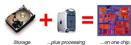
Hard disks might soon be dead. But
what will replace them? Here’s a look at four technologies that
could be called “hard disk killers”.
Holographic Storage
Near – Field Optical Recording Using A Solid Immersion Lens
MEMS – Based Storage
Atomic Storage Using STMs and AFMs
1. Holographic Storage
Holographic Storage has been talked about for a long time;
indeed, the Holographic Versatile Disc (HVD) is being eagerly
awaited by people around the world. This technology user lasers
to record data in the volume of the medium, rather than on the
surface. The idea is not new, but it’s only now that the
technology seems to be getting up to speed.
How does it work? A
laser beam is split in two; the reference beam and the signal
beam (called it so because it carries the data). A device called
a spatial light modulator (SLM) translates 1’s and 0’s into an
optical pattern of light and dark pixels, are arranged in an
array (or pages) of about a million bits.
The signal beam and the references beam intersect in the storage
medium, which is light-sensitive. And at the point of
intersection, a hologram is formed because of a chemical
reaction in the medium, and gets recorded there. (A hologram is
the interference pattern that result when two light waves meet).
For reading the data, only the reference beam is used; it
deflects off the hologram, and a detector picks up the data
pages in parallel. The 1’s and 0’s of the original data can be
read from the data page.
. The device first splits a blue-green argon laser beam into
separate reference and object beams. The object beam, which
carries the data, gets expanded so that it fully illuminates a
spatial light modulator (SLM). An SLM is simply an LCD panel
that displays a page of raw binary data as an array of clear or
dark pixels.
The object beam finally interacts with the reference beam inside
a photosensitive crystal. The ensuing interference pattern--the
substance of the hologram--gets stored as a web of varying
optical characteristics inside this crystal. To read out the
data, the reference beam again illuminates the crystal. The
stored interference pattern diffracts the reference beam's light
so that it reconstructs the checkerboard image of the light or
dark pixels. The image is directed upon a charge-coupled device
(CCD) sensor array, and it instantly captures the entire digital
page. When reading out the data, the reference beam has to hit
the crystal at the same angle that's used in recording the page.
The beam's angle is crucial, and it can't vary by more than a
fraction of a degree. By
varying the angle or wavelength of the reference beam, or by
slightly changing the placement of the medium lots of holograms
can be stored in the volume of the medium.
2. Near-Field Optical Recording Using A Solid
Immersion Lens
Think of a CD or DVD; while recording, the lens focuses the
laser onto a tiny spot on the medium. This spot is tinier for
DVD than for CD, and is even tinier in Blue-ray, for example
Near-field optical recording (NFOR) refers to the extremely
sharp focusing of a laser beam which means an extremely small
distance between the lens and the recording medium. NFOR using a
solid immersion lens (SIL) would be the child of Blue-ray and
HD-DVD and therefore, the grandchild of the DVD.
How does it work?
The density of the data that can be achieved on a disc is
roughly proportional to the square of the numerical aperture
(NA) of the lens, and inversely proportional to the wavelength
of the laser. The NA of a SIL is made very high, and the
achievable data densities are therefore that much higher. In
NFOR using a SIL, the laser is very sharply focused; it
converges at a point within the lens, instead of on the medium.
The air gap between the lens and the medium is just about 25nm!
The photons “tunnel” through the air gap onto the surface of the
medium.
What’s being done?
About half a year ago, Philips researchers reported “significant
process” in developing NFOR. Up to 150 GB of data on a
dual-layer disc would be possible, they said the technology was
several years away from commercialization.
3.MEMS Based Storage
MEMS (Micro-Electro-Mechanical System) is, according to
memsnet.org, “the integration of mechanical elements, sensors,
actuators, and electronics on a common silicon substrate through
micro fabrication technology.” The mechanical elements referred
to here, range in size from a few micrometers to a millimeter.
Actuators are just devices that convert an electronic signal to
a physical action-for example of a MEMS-based storage system to
better explain what MEMS are.
How does it work?
Different MEMS storage system work differently, but we can
describe the concept. Take a look at the figure alongside. This
isn’t a working a working system, but just an example of a
general MEMS storage system. The data “sled” at the top can move
in all three directions; it is spring-mounted over the probe tip
array, an array of mechanical tips that do the reading and
writing. There’s an actuator on each side of the data sled, and
it moves the sled in response to electric currents. Now when the
first bit is written, the sled and the tip array are aligned,
and then the sled moves along one axis while the tips do their
work-writing a 1 or a 0. Note that the sled doesn’t rotate; it
slides. Also note that everything in this arrangement is
mechanical and electronic.
4. Atomic Storage using STMs and AFMs
Take a look at the figure alongside. Notice the “IBM”? It’s not
a photograph, but it depicts what researchers have etched at the
atomic scale each of the hills in an individual Xenon atom! The
thing was produce using an Scanning Tunneling microscope (STM)
operating a few degrees above absolute zero.
How does it Work? An
STM has the ability to give a view of surfaces at the atomic
scale, and research have envisioned the application of the
technique to achieve ultra-high-density storage. The STM has an
ultra-sharp tip placed extremely close to the substrate being
written onto. A voltage applied between the tip and the
substance gives rise to a tunneling current. The tunneling
current depends on the separation between the tip and the
substance. As the tip is moved over the surface, the tunnel
current is monitored, and the position of the tip is changed
such that the current is constants this way, the topology of the
surface can be mapped out. The beauty of STM is that it can be
used not only to map a surface, but also to modify it.
There are difficulties with the STM approach-one is the problem
of maintaining the distance between the tip and the surface at
the angstrom level (an angstrom is 0.1 nm). To overcome these
difficulties, researchers are concentrating more on the Atomic
Force Microscope (AFM). Here, the tip rests on a cantilever
spring. This allows for two things: first, the tip can actually
touch the surface, because of the “bounce” enable by the spring.
Second, by monitoring and controlling the spring, extremely
small force can be sensed as well as applied.
Associate System
Engineer, IBM

Disclaimer : The views expressed in the articles are author’s own. B’Cognizance or IIITA is not liable for any objections arising out of the same. The matter here is solely for academic use only.